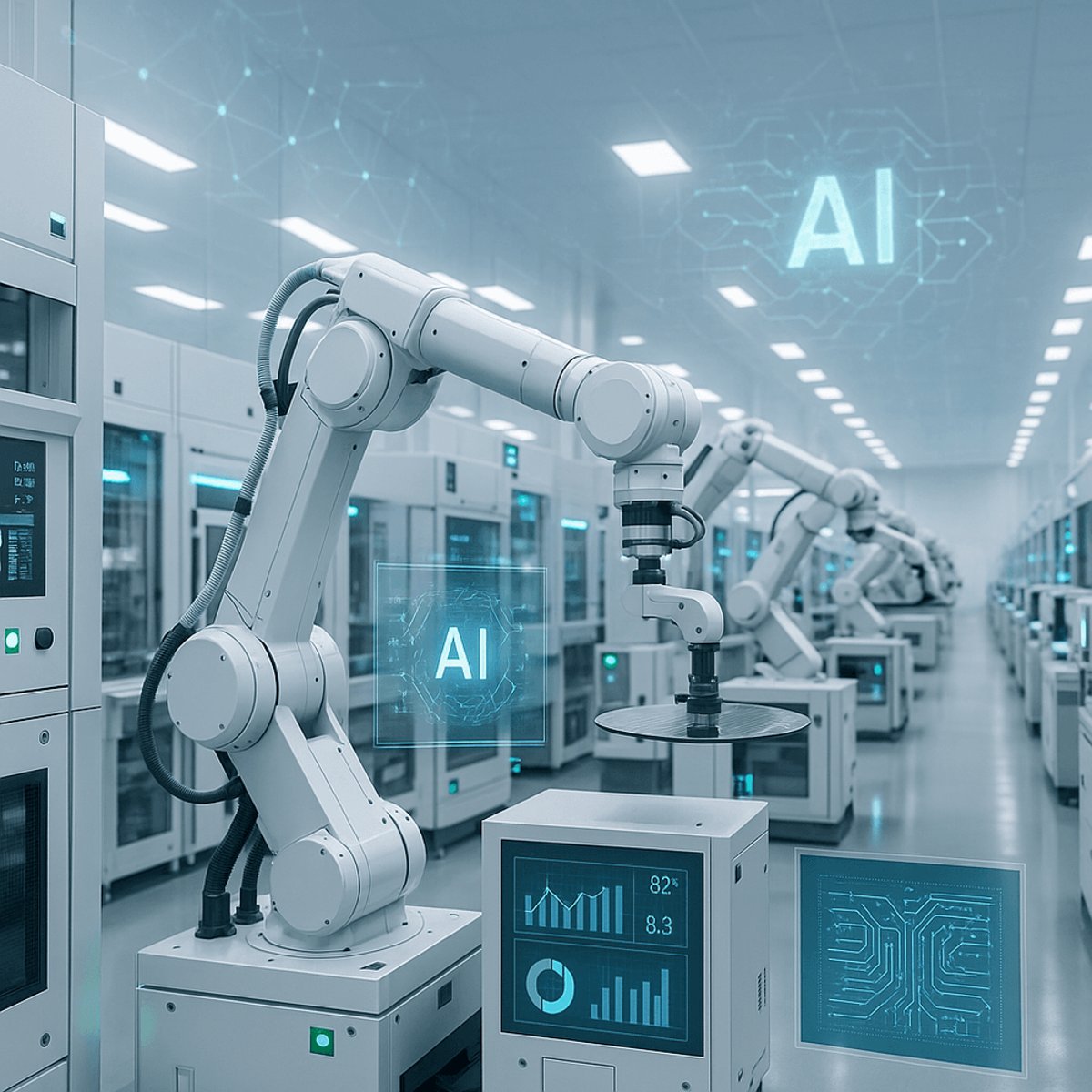
Samsung just announced its most ambitious AI manufacturing project yet - a new AI Megafactory powered by over 50,000 NVIDIA GPUs. This partnership marks a major escalation in the race to AI-driven semiconductor production, potentially reshaping how chips get made worldwide. The scale alone - 50,000 GPUs - dwarfs most enterprise AI deployments and signals Samsung's serious bet on AI transforming manufacturing from the ground up.
Samsung just dropped plans for what might be the world's largest industrial AI deployment. The Korean tech giant announced its AI Megafactory partnership with NVIDIA, deploying more than 50,000 GPUs to completely transform how semiconductors get manufactured. This isn't just automation - it's AI embedded throughout Samsung's entire production pipeline, from initial chip design to final quality control.
The timing couldn't be more critical. As the semiconductor industry faces mounting pressure to produce more advanced chips faster, Samsung's betting that AI can solve manufacturing bottlenecks that have plagued the industry for years. The company plans to integrate AI into every aspect of production - design, process optimization, equipment management, and real-time quality control - creating what they call "a single intelligent network."
This builds on a partnership that goes back over 25 years, starting when Samsung's DRAM powered NVIDIA's early graphics cards. But the scale here is unprecedented. According to Samsung's announcement, the AI Factory will analyze and optimize production environments in real-time, going far beyond traditional factory automation.
The technical specs reveal just how serious Samsung is about this transformation. Using NVIDIA's cuLitho and CUDA-X libraries for optical proximity correction, Samsung has already achieved a 20x performance gain in computational lithography. That's the process that determines how accurately circuit patterns get etched onto silicon wafers - a critical step that directly impacts chip yield and performance.
"We've seen companies talk about AI in manufacturing for years, but this is different," according to industry analysts tracking the semiconductor space. The 50,000 GPU deployment represents one of the largest enterprise AI installations ever announced, putting Samsung ahead of competitors still experimenting with pilot programs.
The partnership also advances Samsung's HBM4 development, with processing speeds reaching 11 gigabits per second - far exceeding the current JEDEC standard of 8Gbps. Built with Samsung's 6th-generation 10nm-class DRAM and 4nm logic, these memory solutions will power the AI applications driving the factory itself, creating a self-reinforcing cycle of AI-powered production.
NVIDIA's Omniverse platform plays a central role, enabling Samsung to build digital twins that visualize entire fabrication operations virtually. These virtual environments can identify anomalies, predict maintenance needs, and optimize production changes before they're applied in the physical world. It's like having a complete virtual replica of Samsung's most complex manufacturing processes.
The implications extend well beyond Samsung's facilities. The company plans to roll out this AI Factory infrastructure to global manufacturing hubs, including its new facility in Taylor, Texas. That means American semiconductor production could benefit from AI optimizations developed in Samsung's Korean facilities, potentially boosting domestic chip manufacturing capabilities.
Samsung's also integrating its proprietary AI models - which already power over 400 million devices - directly into manufacturing systems. Built on NVIDIA's accelerated computing and Megatron framework, these models handle real-time translation, multilingual conversations, and intelligent summarization across production lines.
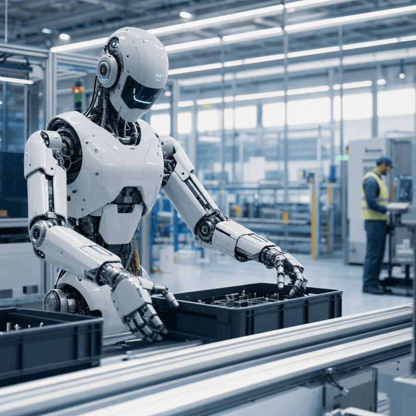
The robotics component adds another layer of sophistication. Samsung's leveraging NVIDIA's RTX PRO 6000 Blackwell Server Edition and Jetson Thor platforms to advance manufacturing automation and humanoid robotics. The goal is robots that can understand their surroundings, make decisions, and operate intelligently in real manufacturing environments.
But perhaps the most intriguing development is Samsung's work on AI-RAN (AI Radio Access Network) technology. Partnering with Korean telecom operators and research institutions, Samsung's building AI-powered mobile networks that could enable robots, drones, and industrial equipment to operate intelligently at the network edge. This technology could be crucial for widespread physical AI adoption across industries.
This announcement comes as the semiconductor industry faces unprecedented challenges. Chip complexity continues increasing while manufacturing costs spiral upward. Traditional approaches to improving yield and reducing defects are hitting physical limits. Samsung's betting that AI can break through these constraints, potentially giving them a significant competitive advantage over rivals still relying on conventional manufacturing approaches.
Samsung's AI Megafactory represents more than just a technology upgrade - it's a fundamental shift toward AI-native manufacturing that could redefine how semiconductors get produced globally. With 50,000 NVIDIA GPUs driving everything from lithography optimization to robotic automation, Samsung's making a massive bet that AI can solve manufacturing challenges that have constrained the industry for decades. If successful, this approach could give Samsung a significant competitive edge while potentially reshaping semiconductor production standards worldwide. The real test will be whether these AI-driven optimizations can actually deliver the promised improvements in yield, quality, and production speed at the scale modern chip manufacturing demands.